The NFM disposes of a wide range of experimental facilities for the synthesis and processing of thin film and surfaces, for the characterization of the synthesized materials and for the determination of their properties.
SYNTHESIS AND PROCESSING OF THIN FILM AND SURFACES.
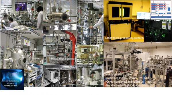
Fifteen reactors working in vacuum, each one with a different function and application possibilities (substrate holders, specific cleaning and processing methods, etc.) are available at the NFM unit. Current processing methods include PVD by e-bam or thermal evaporation, plasma sources for plasma cleaning, PECVD and plasma polymerization, particles beam production, broad ion gun sources, magnetron sputtering devices (DC, AC, pulsed, HIPIMS) etc. Likely, these processing facilities are the most complete in Spain and possibly among the most complete in Europe. Recently, the unit has begun to use other surface processing methods like laser treatment or spin coating. These facilities are still modest, although it is the unit purpose to advance in the incorporation of new methods to develop hybrid technologies involving for example PVD or PECVD plus laser treatment and other procedures.
CHARACTERIZATION AND PROPERTY DETERMINATION TOOLS.
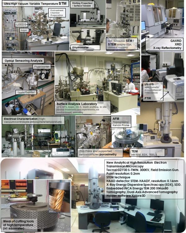
The panoply of techniques available in the unit cover all procedures required for a thorough characterization, chemical, structural and microstructural, of the prepared layer materials. Equipment is available at the unit (e.g., AFM, XPS), the ICMS (Raman, FT-IR, electron microcopies, XRD) and the services of the University of Seville, these latter including the most modern apparatus in the market. Occasionally, the researchers make use of special tools available in the University of Malaga (environmental SEM), the Univ. of Extremadura (SIMS) and the Uni. Pablo de Olavide (SEM with electrical probes). Researchers of the unit are recognized experts in methods such as X-ray photoemission, transmission electron microscopy, proximity probe microscopy and others. It is also noteworthy that the unit researchers make also use of medium and large facilities like synchrotron (XAS, environment photoemission), or ion accelerators for RBS analysis of thin films (the CNA sponsored by the Univ. Seville is 200 meters separated from the ICMS). The unit is also well-equipped for the determination of functional properties based on the the optical (UV-vis spectroscopy, ellipsometry), electrical (four probe methods, capacitance characterization, etc.), surface wetting and tribological performance of thin film and surfaces.
APPLICATIONS AND DEVICE PROTOTYPING.
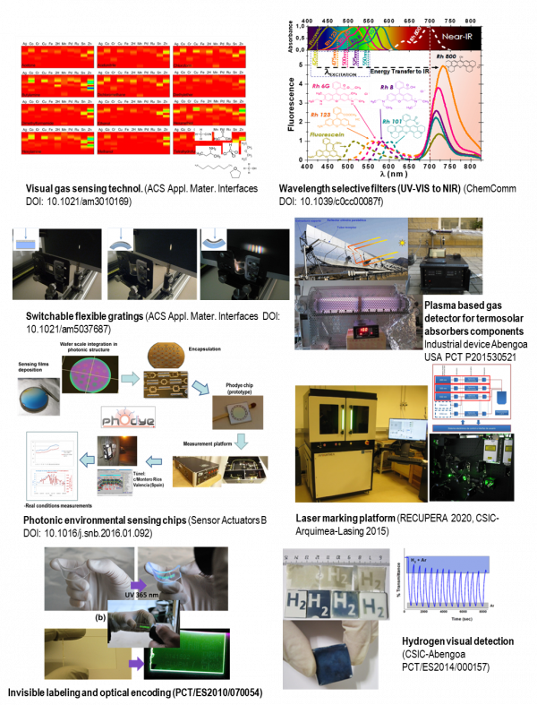
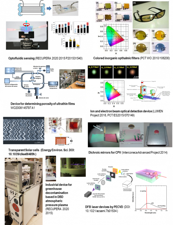
Unlike the availability of most important tools and procedures for the processing and characterization of thin films and surfaces, the unit has a certain shortage in robust procedures for the prototyping of final devices where to test final functionalities. This is in part due to the natural evolution of a research unit, initially focused on the synthesis and characterization of new surface materials and nanostructures, towards applications driven technologies. The NFM unit is moving towards application driven research topics. Despite the shortage of means, steps have been already done in relation with an incipient use of lasers for surface nanostructuration, (1) the fabrication of simple microfluidic and optofluidic devices (2) or some basic electrochemical devices (3).
References
1.- V.J. Rico et al. ACS Appl. Mater. Interf. 8 (2016) 24880
2.- M. Oliva-Ramírez et al. Sens. Actuat. B: Chemical 256 (2018) 590
3.- P. Salazar et al. Electrochim. Acta 193 (2016) 24.